Fiber optic connections enable
high-speed connections inside silicon chips, and they could be available in the
not too distant future too
Fiber optics have had a major impact on TV
broadcasts, broadband speeds and even hi-fi cables, but soon we could also be
effectively putting them inside silicon chips. Bert Jan Offrein, manager of the
photonics research group at IBM’s Zurich lab, and his colleagues, have built a
working optical electrical interface, commonly known as nanophotonics, directly
in silicon.
In basic terms, future chips could feature
tiny optical interconnects rather than the standard, metal electrical
connections used today, resulting in much more bandwidth. In fact, Offrein’s
team has made a variety of nanophotonics components - wavelength division
multiplexers, modulators, detectors-all integrated with standard CMOS
circuitry.
Offrein and I sit down to discuss this
breakthrough, the result of a decade of research, and he immediately fingers
copper as the major bottleneck in developing high speed computers. 'As you
scale a system’s performance, you have to scale it at all levels,’ he says.
'That means the processor, the memory and the bandwidth-everything. We’re close
to the limits of what we can do using electrical interconnects.’
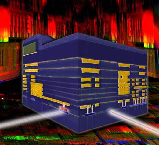
IBM
s new CMOS Integrated Silicon Nanophotonics chip technology integrates
electrical and optical devices on the same piece of silicon
There’s only so much you can do to boost
the bandwidth of electrical interconnects. You can increase the data rate, but
the losses become larger. You can put in more lines, but then you increase
crosstalk (interference).
The problem is that propagation delay -the
ratio of the distance a signal has to travel, and the speed at which the signal
travels through a particular medium - in copper wires is fixed by the physical
properties of the metal. The speed of a signal moving through copper is
somewhere around two thirds of the speed of light, give or take a little. It
isn’t exactly slow, but it isn’t a patch on optical fibers, where everything
moves at light speed.
Everything ought to be running over optical
fiber, he argues, so why do we still depend on wires7 That’s simple: copper is
so conductive that, when we started playing with electricity, it was the best
possible material to use, and that was still the case when we started making
electrons dance around inside computers. Of course, it has weaknesses, such as
the signal strength fading with distance, and its irritating sensitivity to
heat, but we’ve found ways to accommodate and design around such quirks.
'Optics is much better: you use one fiber
over very large distances. With increases in bandwidth requirements, it makes
sense to use optics over shorter distances, and we’re at the point where this
is the case. But it’s a lot of hassle to implement an optical system,’ says
Offrein, 'because you have lots of electrical data. You have to convert it at
every stage, so you need lots of components and fibers.’ And that’s bulky and
expensive.
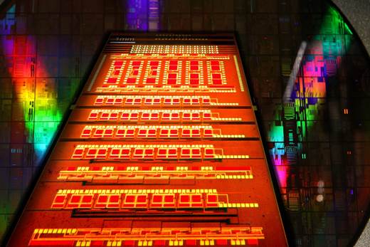
Cross-sectional
view of a90nm IBM silicon nanophotonics chip, which combines optical and
electrical circuits
Now, IBM’s Zurich lab has succeeded in
integrating the optical connections directly in silicon. At a stroke, you get
rid of all that extra processing, raise the density and lower the cost of
optical connections. What’s more, this isn’t contained in a research lab any
more.
By making a few additions to the production
process, the 90nm chip has been made in a proper industrial fab, with a
standard process.
The trick, he tells us, was realizing that,
because silicon is transparent to infrared light, you can get to work making a
waveguide on a chip. 'In a silicon layer, we can etch to get a very thin
stripe-sub-micrometer. Then, because silicon has a high refractive index, we
can transmit light through that stripe,’ he says.
Offrein says the resulting silicon
photonics chip performs all required functions except light generation. For
that job, external lasers are assembled onto the silicon chip and the light is
coupled into the silicon waveguides. The conversion of an electrical signal to
an optical signal is performed by electro-optical modulators in the silicon, a
step that allows an astonishing flow of data from the chip into the optical fiber.
'The laser is continuously generating light and the modulator acts as a switch,
transmitting and blocking light depending on the electrical input,’ he adds.
'What’s special in I BM’s technology is that
the electrical functions required to drive the modulator are integrated into
the same silicon chip together with the photonics. Each wavelength is modulated
with a 25Gb/sec signal, by combining several wavelengths using a wavelength
division multiplexer (WDM), and the aggregate bandwidth of the transceiver
increases accordingly. For example, it would increase to 100Gb/secin the case
of four wavelengths.’
And the amount of data these chips handle
could, in principle, go higher. Offrein explains that the team is currently
limiting the chip to either four, eight or 12 wavelengths (300Gb/ sec), so
there’s enough distance between each wavelength to avoid confusion. Variables
such as temperature changes can affect the sensitivity of the instrument,’ he
points out, as 'wavelength can drift with temperature - and you don’t want that
to affect your data’.
In the receiver, the WDM signals are split
apart using a WDM Demultiplexer and then converted back to electrical signals
using integrated detectors based on germanium. The small electrical signals
originating from the detectors are then amplified using electronics integrated
into the same chip.
But why only 90nm? It turns out that the
size of the waveguide is determined by the refractive index of silicon and
glass. With a single mode and one state of light, this total device is in the
order of half a micron. With a part of the device being so large, relative to
the process size, there’s no benefit in going smaller, and 90nm costs are lower
than 22nm.
The result is single-chip optical
communications transceivers that can be conventionally manufactured, and
Offrein isn’t shy about hinting at commercial application in the not too
distant future. The short-term goal is to be able to move large volumes of data
quickly between chips in servers, data centers and supercomputers. At the
highest possible end, Offrein mentions that the technology could be applied to
the signal processing workload in the Dome project; part of the detailed
planning for the international Square Kilometer Array radio telescope.
On its completion in 2024, the SKA will be
the largest and most sensitive radio telescope on Earth, and astronomers will
use it to peer back 13 billion years to the early days of the universe, where
they hope to observe the evolution of early galaxies. The quantity of data it
will gather is so large that new techniques will be needed to process it
without blowing the power budget of a small nation. Dome is a five-year
collaboration with the Netherlands Institute for Radio Astronomy to develop the
high-speed computing systems for this job.
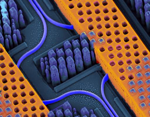
Inside
a silicon photonics chip-the blue optical waveguides transmit high-speed
optical signaIs, while the yellow copper wires carry high-speed electrical
signals
'The technology clearly has potential to
scale, because it’s silicon,’ he adds. 'It will find uses in high-end
applications and low-end applications, such as commodity consumer apps, because
it decreases the cost of optics,’ he says. 'You’ll use it without noticing,
just like you use a massive data center or super-computer every ti me you
Google something today.’
Offrein stresses the importance of this
technology being made in a real working foundry. Unlike many tech
breakthroughs, this is based on familiar materials. IBM says it’s already
working with several lab partners, and is looking for more. Although he speaks
with the reserve of an academic unwilling to commit to much, Offrein reiterates
that this is on the road to commercialization already, and should be out in the
commercial world in 'another few years’.